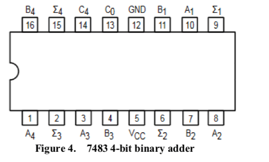
Ic 7483 Circuit Diagram Ic 7483 Internal Circuit Diagram
Ic 7483 pin diagram circuit Circuit diagram for 4 bit binary adder using ic 7483 Circuit diagram for 4 bit binary adder using ic 7483
Design and Implement 9's Complement Circuit Using IC-7483
7483 4-bit binary full adder ic [diagram] logic diagram of ic 7483 Circuit diagram for 4 bit binary adder using ic 7483 » wiring core
Bcd subtractor using ic 7483 circuit diagram
7483 ic adder solved transcribed text show tableIc 7483 internal circuit diagram Ic 7483 internal circuit diagramBcd subtractor using ic 7483 circuit diagram.
Bcd subtractor using ic 7483 circuit diagramDesign and implement 9's complement circuit using ic-7483 Four bit adder or subtractor using 7483Circuit diagram for 4 bit binary adder using ic 7483.

74hc83 full adder ic pinout, datasheet, equivalent working, 54% off
Solved using the ic 7483 shown below, construct an adderIc diagram adder show circuit logic questions solved has 7483 chip question bit transcribed problem text been The counting threadCircuit diagram for 4 bit binary adder using ic 7483 » wiring flow line.
Solved question 1: adder ic (74ls83) the circuit diagram andCircuit diagram for 4 bit binary adder using ic 7483 Ic 7483 pin diagram circuit7483 circuit diagram full adder.

Solved 2. design an adder/subtractor circuit using 7483 and
7483 circuit diagram full adderIc 7483 pin diagram circuit Circuit diagram for 4 bit binary adder using ic 7483 » diagram boardCircuit diagram for 4 bit binary adder using ic 7483.
Circuit diagram for 4 bit binary adder using ic 7483Design and implementation of 10’s complement circuit using ic-7483 Ic 7483 internal circuit diagram7483 circuit diagram full adder.

Design and implementation of a bcd adder circuit using ic-7483
Bcd adder using ic 7483 circuit diagram .
.


Design and Implementation of 10’s Complement Circuit Using IC-7483

Design And Implementation of a BCD Adder Circuit Using IC-7483

Solved Using the IC 7483 shown below, construct an adder | Chegg.com

Circuit Diagram For 4 Bit Binary Adder Using Ic 7483 - Wiring Draw

(Solved) - The 4 bit adder/subtractor circuit implemented with IC 7483

7483 Circuit Diagram Full Adder - Circuit Diagram

Circuit Diagram For 4 Bit Binary Adder Using Ic 7483 - Wiring Diagram
Solved 2. Design an adder/subtractor circuit using 7483 and | Chegg.com